
Skip links

Guides

How to Patent Semiconductor Chip Design:

Building an IP Strategy for the Most Competitive Industry on Earth

Get In Touch

651-256-9480

Table of Contents

Semiconductor chip design is one of the most patent-dense fields in technology. Global semiconductor patent filings jumped 22% in the most recent reporting period, rising from roughly 66,400 to over 80,800 applications. Semiconductor technology has topped the list for the most granted patents in the last three years. And with the CHIPS and Science Act pushing $52.7 billion into domestic chip R&D and manufacturing, the pace of innovation and the urgency of protecting intellectual property (“IP”) in this technological space are only accelerating.

But patenting chip design is not straightforward. A single integrated circuit can involve patentable circuit architecture, a protectable chip layout under the Semiconductor Chip Protection Act, copyrightable embedded software, and manufacturing processes that may be best kept as trade secrets. Knowing which form of IP protection applies to which aspect of your design, and how to layer them together, is the difference between a portfolio that actually protects your competitive position and one that leaves critical gaps.

At Gallium Law, we work with semiconductor companies and chip designers at every stage, from startups developing novel architectures to established firms building out their patent portfolios ahead of licensing, fundraising, or M&A. This guide covers what you can and cannot patent, and how the different forms of IP protection fit together for chip design.

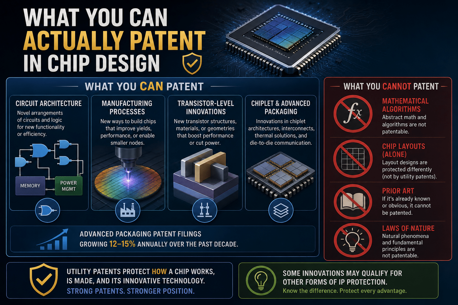
What You Can Actually Patent in Chip Design

Not everything in a semiconductor chip is patentable. A utility patent protects a novel, non-obvious, and useful invention. In the semiconductor context, that covers a lot of ground.

Circuit Architecture and Logic Design

Novel circuit architectures are among the most valuable semiconductor patents. If your chip uses a new arrangement of logic gates, a novel signal processing pathway, a unique memory cell structure, or an innovative approach to power management, those architectural decisions can be patented. The claim does not need to cover the entire chip. A patentable innovation can be a single functional block within a larger design, as long as it meets the novelty and non-obviousness requirements. Our overview of the patent process from idea to application walks through how the process works from initial concept through filing.

Manufacturing Processes

How a chip is fabricated can be just as valuable as what the chip does. Novel etching techniques, doping processes, lithography methods, deposition sequences, and packaging innovations are all patentable. Process patents are particularly powerful in semiconductors, because they can be difficult for competitors to design around. If your fabrication process produces better yields, tighter tolerances, or enables smaller process nodes, that process is worth protecting.

Transistor-Level Innovations

Advances in transistor design, from finFETs to gate-all-around architectures, have driven much of the semiconductor industry’s recent progress. If you have developed a novel transistor structure, a new approach to gate geometry, or an innovative material stack that improves performance or reduces power consumption, those innovations sit squarely within patentable territory.

Chiplet and Advanced Packaging

This is one of the fastest-growing areas of semiconductor patenting right now. Advanced packaging patent filings have grown by 12-15% annually over the past decade. Chiplet architectures, which disaggregate a monolithic chip into smaller, independently manufactured blocks connected through advanced packaging, involve novel interconnect designs, thermal management solutions, and die-to-die communication protocols. Each of those is potentially patentable.

What You Cannot Patent

You cannot patent a mathematical algorithm or a law of nature. You cannot patent a chip layout purely as a layout. That is a different form of protection (more on that below). And you cannot patent something that is already known in the prior art, or that would be obvious to a person skilled in the field. The prior art landscape in semiconductors is enormous, which makes a thorough search before filing essential. Understanding how design patents differ from utility patents clarifies where utility patents apply versus other forms of protection, which matters when you are deciding what to patent and what to protect through other means.

Mask Work Protection: The IP Right Most Chip Designers Overlook

Congress passed the Semiconductor Chip Protection Act (SCPA) in 1984 specifically because existing IP law did not adequately protect chip designs. Traditional patent law covers inventive concepts but not the specific topographical layout of an integrated circuit. Copyright covers creative expression, but not functional designs. Trade secret law collapses the moment someone decaps your chip and photographs the layers.

The SCPA created a sui generis (one of its kind) intellectual property right called mask work protection. A mask work is the series of related images that define the topography of a semiconductor chip: the arrangement of transistors, capacitors, resistors, and their interconnections across the layers of the integrated circuit. Registration gives you 10 years of exclusive rights against anyone who copies that specific layout.

How a Mask Work Differs from a Patent

A patent protects the inventive concept regardless of how it is implemented. If you patent a novel circuit architecture, no one can build that architecture in any physical form without your permission for 20 years. Mask work protection is narrower. It protects your specific topographic implementation of a design, not the underlying concept. If a competitor designs a functionally equivalent circuit using a different layout, mask work protection will not stop them. But if they photograph your layers and reproduce them, it will.

The two protections complement each other. A patent covers the broad inventive concept. Mask work covers the specific physical expression of that concept in silicon. For chip designs that involve both novel architecture and significant layout engineering, filing for both creates a stronger defensive position than either one alone.

Registration Requirements

Mask work registration is handled by the U.S. Copyright Office, not the USPTO. You must file within two years of the first commercial exploitation of the chip. The registration requires a deposit of the mask work, and if portions contain trade secrets, you can file redacted versions while keeping unredacted copies on record. The filing fee is modest compared to a patent application, and the process moves faster. If you have chips in production and you have not filed for mask work registration, you may be leaving protection on the table.

Building a Layered IP Strategy for Semiconductor Technology

The most effective semiconductor IP portfolios use multiple forms of IP protection working together. A single chip design can involve all of the following:

  1. Utility patents covering the novel circuit architecture, transistor innovations, or manufacturing processes. 
  2. Mask work registration covering the specific topographic layout. Trade secret protection for proprietary fabrication recipes, yield optimization techniques, and design rule databases that never need to be disclosed. 
  3. Copyright for any embedded firmware or software. 
  4. And potentially design patents for distinctive physical features of the packaged chip if they serve an ornamental function.

The key is understanding which form of protection applies to which aspect of your technology, and making sure nothing falls through the cracks. We see semiconductor clients who have strong patent portfolios but have never filed a mask work registration, or who have excellent trade secret practices around their manufacturing processes but have not patented the product those processes produce. Our patent prosecution and strategy services are built around this kind of layered approach, where every protectable aspect of your technology gets the right form of coverage.

Provisional Applications and the Race to File

The semiconductor industry moves fast. Design cycles are measured in months. If a competitor files a patent on an architecture you developed independently, the fact that you had the idea first does not matter under the current first-to-file system. Whoever gets to the USPTO first owns the priority date.

Provisional patent applications exist specifically for situations like this. A provisional filing establishes your priority date, gives you 12 months to file the full non-provisional application, and costs a fraction of what a complete filing requires. For semiconductor design teams iterating on architecture or process innovations, filing provisional applications as key milestones are reached is a way to lock in priority without waiting for the design to be finalized. Our comparison of provisional vs. non-provisional patent applications explains the strategic differences between the two and when each makes sense.

There is a trap here, though. A provisional application only protects what is actually described in the filing. A vague or incomplete provisional that does not adequately disclose the invention will not hold up as prior art if someone else files a more detailed application later. The provisional needs to be substantive enough to support the claims you will eventually file in the non-provisional. Cutting corners on the provisional to save time or money can cost you the priority date you were trying to secure.

The CHIPS Act and Why Patent Strategy Matters More Now Than Ever

The CHIPS and Science Act has changed the landscape for semiconductor IP in the United States. With $52.7 billion flowing into domestic chip R&D and manufacturing, the number of companies developing novel semiconductor technology in the U.S. is growing. More companies means more innovation, which means a denser patent landscape and more potential conflicts.

For companies receiving CHIPS Act funding, demonstrating a strong IP portfolio is both a competitive advantage and, in many cases, a condition of continued funding. Investors and government stakeholders want to see that the technology they are backing is protected. A well-constructed patent portfolio signals that the company takes its competitive position seriously and has enforceable rights in the innovations it is developing.

The geopolitical dimension matters too. Semiconductor patents are no longer just commercial tools. They are strategic assets in an industry where supply chain security is a national priority. Companies that build strong, defensible patent portfolios around their chip designs are better positioned for partnerships, licensing revenue, and acquisition interest in a market where governments are actively investing in domestic semiconductor capability. IP due diligence is increasingly important in semiconductor transactions, and the strength of the IP portfolio is often the deciding factor.

Mistakes That Weaken Semiconductor Patents

Semiconductor patents fail for predictable reasons. Knowing what those are saves time, money, and the kind of strategic exposure that shows up years later when you try to enforce a patent and discover it does not cover what you thought it covered.

Claims That Are Too Narrow

A patent claim that describes your specific implementation in exhaustive detail might be easy to draft, but it is also easy for a competitor to design around. One small change to a parameter, a material substitution, or a different transistor count, and they are outside your claim scope. Effective semiconductor patent claims balance specificity (enough to distinguish from prior art) with breadth (enough to capture meaningful variations). Understanding the doctrine of equivalents in patent infringement helps here, but it is far better to draft claims that capture the competitive landscape from the start than to rely on legal doctrines to extend them after the fact.

Disclosing Before Filing

Publishing a paper, presenting at a conference, or even sharing details with a potential partner without an NDA can start a clock that jeopardizes your patent rights. Under U.S. law, you have a one-year grace period after public disclosure to file, but many foreign jurisdictions have no grace period at all. A conference presentation about your novel chip architecture can destroy your ability to patent that architecture in Europe or Asia. Our guide on public disclosure without IP protection explains why this is one of the most common and costly mistakes semiconductor startups make. And before sharing anything, make sure you understand the rules around protecting your idea before your patent is filed.

Ignoring the Prior Art Landscape

Semiconductors have one of the densest prior art landscapes of any technology sector. Filing a patent application without conducting a thorough prior art search risks wasting prosecution time and fees on claims that the examiner will reject based on existing publications and patents. Worse, it risks building a product that infringes someone else’s patent. A freedom-to-operate analysis before you commit to a design direction, and a patentability search before you commit to a filing strategy, are both worth the investment.

Protecting What You Build in Silicon

Semiconductor chip design sits at the intersection of multiple forms of IP protection, and no single filing covers everything. Patents protect your inventive concepts. Mask work registration protects your physical layout. Trade secrets protect what you never need to disclose. The companies that build the strongest positions are the ones that use all of these tools deliberately, with a strategy that accounts for how each form of protection complements the others.

At Gallium Law, we work with chip designers and semiconductor companies to build IP portfolios that match the complexity of the technology they are developing. Whether you are filing your first provisional application on a novel architecture, building out a patent portfolio ahead of a funding round, or evaluating whether your existing coverage has gaps, reach out and let us build a strategy that protects your work at every layer.